The Effect of Packaging on the Light Output of IREDs
When an IRED Is forward biased a percentage of the injected carriers which recombine in the vicinity of the P-N junction result in the generation of photons. Not all of the generated light is able to emerge from the interior of the IRED chip due to these power loss mechanisms:
1. absorption
2. Fresnel losses
3. internal reflection
Mounting the IRED die in a package not only serves to protect it from a potentially hostile environment but can also be used to back at the interface between the two materials. This reflected power is called the fresnel loss. As photons travel outward through the chip from the junction region there is a probability that absorption will take place. The longer the travel distance the greater the internal absorption. This is the reason that smaller IRED sizes exhibit the highest power conversion efficiencies.
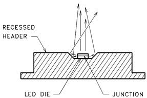
Because the P-N junction extends to and is exposed at the four sides of the chip, a large percentage of the total light output is emitted from these sides. By mounting the IRED chip in a contoured cavity it is possible to collect a larger percentage of this side emitted light and reflect it upwards.
When light travels from a material with index of refraction n1 into a medium with index of refraction n2 some of the light is reflected back at the interface between the two materials. This reflected power is called the fresnel loss.
For normal incidence, the Fresnel loss efficiency factor is given by:
ηFR = 4 / (n22 + n2 ⁄ n1 + n1 ⁄ n2)
where:
n1 = index of refraction of the IRED
n2 = index of refraction of the material surrounding the chip
For a GaAs IRED chip emitting directly into air:
ηFR = 4 / ( (1 + 1 ⁄ 3.62) + 3.62 ⁄ 1) = 82%
Hence only 82% of the light reaching the chip’s surface exits the chip. More light power can be extracted from the chip by coating it with a matching material whose index of refraction lies between that of the chip’s and that of air. When an “index matching” material is used the transmission efficiency can be increased to over 90%. Optimum transmission efficiency is achieved when the index matching material used has an index of refraction of √n1n2.
Loss also occurs due to total internal reflection. If photons of light are incident to the chip’s surface at angles greater than the critical angle they are reflected back into the crystal.
θC = sin-1(n2 ⁄ n1)@ 16° (for GaAIAs)
where:
θC = critical angle
n1 = index of refraction of the LED
n2 = index of refraction of the material surrounding the chip
This situation can be improved by coating the LED chip with a plastic encapsulant.

θC = sin-1(nx ⁄n1) = sin-1(1.3 ⁄3.62) ≅ 21°
Lenses, incorporated into the IRED package, can be used to increase the useable forward power intensity by focusing the light emitted by the IRED.

The lenses used on metal/glass hermetic packages are made from a glass whose thermal coefficient of expansion closely matches that of the Kovar (iron-nickel-cobalt alloy) package. For IREDs which use leadframe construction, lenses can be made an integral part of the cast of molded package.
The lenses used on IRED are not precision ground. Expect variations in the light pattern from unit to unit due to lens quality, variations in chip placement, shape of the reflector cavity, number and type of material interfaces, and distance from the lens to the IRED chip. The glass lens used in hermetic packages is formed by melting and reflowing a cut glass disc. The overall dimensions and geometry of this reflowed lens show considerable variation. They do not have closely repeatable optical geometry. The focal point, direction, and uniformity of the emitted beam of light show significant variation from unit to unit.
Plastic IREDs have only one optical surface in the lens system. The shape of this lens is controlled by the casting mold or transfer mold. The optical characteristics are more uniform from unit to unit. So, plastic IREDs have a more consistent beam pattern than hermetic IREDs.
IREDs of plastic/leadframe package design have two fewer dielectric interfaces than do IREDs in hermetic packages. As a result plastic packages generally deliver up to 50% more useable focused power than hermetic packages.
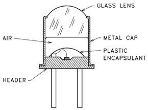
Hermetic Package

Plastic/Leadframe Package
IREDs of plastic/leadframe package design have two fewer dielectric interfaces than do IREDs in hermetic packages. As a result plastic packages generally deliver up to 50% more useable focused power than hermetic packages.
Article based on Application Notes from Excelitas Technologies Photometric and Radiometric Terms application note
Heard on the Internet
Imagination is more important than knowledge.
Albert Einstein


