Discrete Chips - An Alternative Solution to Space Problems
Space restrictions may preclude the use of packaged detectors or emitters in some applications. In these cases the use of
discrete chips might be appropriate because of their small size.
Excelitas offers IREDs and phototransistors in unpackaged die form—ready for hybrid assembly. Chips are supplied loose in vials, in waffle pack chip carriers, or as probed and inked wafers.
Conductive silver epoxy is commonly used for die attach. This method involves dispensing tightly controlled amounts of the epoxy either manually or with automatic equipment. The chip is placed on the epoxy which is then cured at moderate
temperatures.
Connections are made to the metallized contact pads on the top surface of the chip by bonding very fine wires of aluminum or gold from these pads to the package. Typically, thermosonic ball or ultrasonic wedge wire bonding is used. After wire bonding, the chip must be protected from the environment by either sealing it within an appropriate housing or by coating the chip with a clear epoxy or silicone designed for coating semiconductor die. This prevents moisture and contaminates from attacking the chip and wirebonds.
Excelitas offers assembly services for those customers who are not equipped for hybrid circuit manufacturing.
Detector Chips (Dice)
Excelitas’s stock chips are 100% probed for dc current gain, dark current, collector & emitter breakdown voltages, and collector-emitter saturation voltage. Excelitas can also provide special testing to meet your custom requirements.
Emitter (E) and Base (B) aluminum metallized bond parts are provided on the top surface of every phototransistor and photodarlington chip. Some devices also have a collector bond pad on the top surface of the die. For all chips, contact to the collector can be made through the backside of the die, the entire surface of which is metallized with nickel.
Custom single and multichannel detectors can be tooled if stock devices are unable to meet the requirements of your application.
Emitter (IRED) Chips
Excelitas’s stock IRED chips are sample probed for forward voltage at a given current drive, reverse leakage current, and power output. Light output cannot be measured for individual chips while they are in wafer form.
Anode contact is made through the backside (bottom) of the chip. Cathode contact is available through the bonding pad(s) on the top surface. A gold metallization system is employed on both the top and bottom surfaces.
Silver conductive epoxy is recommended for die attach.
Thermosonic gold ball bonding is recommended for the top contact.
Special note on die attach epoxy “slop”. Remember: all high efficiency output IR emitting dice have an electrically exposed PN junction that appears on all four sides of the die. Conductive epoxy placed or “slopped” over the P-N junction can cause a total, partial, or even a time-varying electrical short circuit of the IRED die.
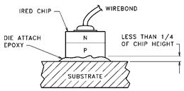
Good Die Attach
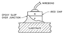
Bad Die Attach
Always use very small amounts of die attach epoxy. Keep the maximum epoxy height less than 1/4 of the height of the IRED chip.
Article based on Application Notes from Excelitas Technologies Photometric and Radiometric Terms application note
Heard on the Internet
Imagination is more important than knowledge.
Albert Einstein


